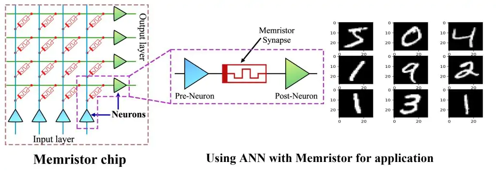
VINIF.2023.DA130 – Development of switching materials, design and fabrication of memristor based chips for applications in artificial neural networks

project manager image
Principle Investigator
Assoc.Prof. Pham Kim Ngoc
Host Organization
University of Science, Vietnam National University - Ho Chi Minh City

The project is implemented with the goal of successfully manufacturing memories that store data through different states of resistance values, known as resistive memory. The outstanding feature of this memory is the ability to change the storage state quickly according to the received voltage signal. This is an important feature that makes it possible to simulate the behavior of biological synapses. On this basis, the team will build an artificial neural network with resistive memory where neurons connect and store their communication information. Create an artificial neural network capable of storing distributed information instead of having to transmit it to external memory DRAM or Flash.
With the goal of basic, application-oriented research, the group conducts research with three specific goals:
• Successfully develop material systems applied to resistive memory, combined with theoretical calculations to evaluate the mechanism and control the operation of components effectively.
• Fabricate a memory chip structure with an integration density from 16 to 4096 memory cells and fabricate an electronic chip circuit with a memory chip acting as an artificial synapse.
• Develop algorithms and deploy them to be applied to recognize images, writing, faces… based on the in-memory computing architecture of the manufactured memory components.

project manager image
Principle Investigator
Assoc.Prof. Pham Kim Ngoc
Host Organization
University of Science, Vietnam National University - Ho Chi Minh City

Tags

Expect Progress
01/11/2023
31/10/2024
Phase 1

– Manufacture memory structure using metal oxide materials and investigate various fabrication parameters.
– Investigate the structure, composition, surface morphology, and resistive switching properties of materials using experimental methods and theoretical calculations.
– Collect a dataset for grayscale image classification (e.g., MNIST). Preprocess for appropriate resolution matching memory chip (stage 3), preprocess for pixel intensity matching memory resistance (stage 1).
– Design an artificial neural network with weight values within the resistance range of the memory fabricated in Content 1, with a structure (number of neurons) compatible with the results of Content 3 (memory network).
– Develop a mathematical model of memories based on experimental properties.
– Draft and submit to international journals, write descriptions and submit patent applications domestically.

31/10/2025
Phase 2

– Continue manufacturing memory structures using metal oxide materials and investigating various fabrication parameters.
– Continue studying the structure, composition, surface morphology, and resistive switching properties of materials using experimental methods and theoretical calculations.
– Perform simulations of the artificial neural network results and evaluate the prediction accuracy on a computer. Estimate prediction errors in cases of memory with errors and a certain percentage of non-functioning memory in the memory network.
– Design and manufacture a control circuit board integrating analog-to-digital converters (ADC), digital-to-analog converters (DAC), amplifiers, microcontrollers connected to a computer via USB port. The circuit board is programmed to perform the complete neural network computation process on the memory chip.
– Design and simulate memory chips on a large scale.
– Draft and submit to a Q1 journal.

31/10/2026
Phase 3

– Survey, evaluate, and optimize the performance of components used in artificial neural joint implants.
– Implement the connection of the memory network with the PCB control circuit. Write firmware to control the forward propagation and backpropagation learning processes through the memory network.
– Optimize the neural network structure, prediction processes, and training to achieve the highest computational efficiency on energy consumption.
– Build and train fully connected ANN networks with a suitable structure for the memory chip, operating with the dataset obtained from Content I.3. Each neural network has weight values compatible with achievable memory resistances.
– Manufacture memory chips.
– Integrate electronics, firmware software allowing communication with the manufactured memory chip, and implement an artificial neural network application.
– Draft and submit to international journals, write descriptions, and submit international patent applications.

Tags